
 Search


(Image credit: Intel)
-
Facebook -
X -
-
-
Pinterest -
Flipboard -
Email
Intel has published a patent to integrate MicroLEDs directly into a CPU package. Aside from communication functions, Intel lists many possible uses, including using multi-colored lights to light up the wording on a processor. The patent, filed in 2022 but only published earlier this month, describes embedding a MicroLED into the package by using a glass substrate and through-glass vias (TGV), connecting directly to a die for power and signal routing. The patent says the purpose of the LEDs is "either aesthetic components of the electronic device or to indicate certain operations being performed by the electronic device."
As is the case with any patents, the purpose of embedding MicroLEDs into a chip is left open-ended. However, Intel interestingly calls out implementing MicroLEDs into a CPU, specifically, and provides several examples of how the tech might be used. The patent says the processor "may operate the micro LEDs so that the micro LEDs visually indicate that certain functions are being performed by the processor or simply for aesthetic effects."
In one part of the patent, Intel describes the LEDs being used to "light up wording across a central processing unit," suggesting some sort of read-out available directly on the CPU. How that would work on a standard processor with a heatsink atop remains an open question. In addition, the patent explicitly calls out that the LEDs can be different colors depending on the implementation. That could mean something more akin to RGB memory than a diagnostic readout. The patent leaves room for both designs.
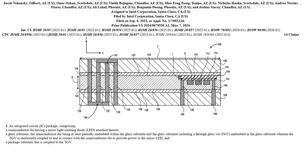
(Image credit: Intel)
You can see the main drawing for the patent above. In the middle is the glass substrate, sandwiched between two layers of package substrate. A semiconductor die is partially embedded within the glass substrate, leaving just the back surface of the die exposed; however, the patent says the die can be fully embedded in other implementations. The LEDs are connected directly to the semiconductor die, or through nanowires, and TGVs deliver power and signal to the semiconductor die through the glass substrate.
Intel says it builds the package with two layers of silicon nitride, which are formed on the package substrate surface and then attached to the glass substrate. Intel has been working through glass substrates for over three years now, as Intel claims it has 10 times better interconnect density than organic substrates.
The main patent drawing only shows a single IC, though the patent notes that's simply shown "for clarity." A finished product implementing this technology "will have an array or arrays of micro LEDs on one or more IC packages." So, given an ambitious-enough design, Intel could implement multiple LED-based functions directly into the processor.
Patents aren't products, and that's always an important reminder. Intel filed this patent over four years ago, and it's just now being published. Whether we actually see MicroLEDs embedded in a processor remains an open question. However, Intel has laid the groundwork to do something like that in the future.

Follow Tom's Hardware on Google News, or add us as a preferred source, to get our latest news, analysis, & reviews in your feeds.

-
 C114 Communication Network
 -
 Communication Home
