

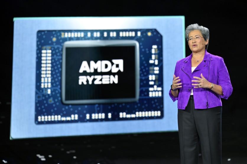
AMD Chair and CEO Dr. Lisa Su delivers a keynote address at CES 2023 at The Venetian Las Vegas on January 04, 2023 in Las Vegas, Nevada. CES, the world's largest annual consumer technology trade show, runs from January 5-8 and features about 3,100 exhibitors showing off their latest products and services to more than 100,000 attendees. David Becker/Getty Images
Three weeks from today, AMD CEO Dr. Lisa Su will take the stage at San Francisco's Moscone Center for Advancing AI 2026, the company's annual flagship AI showcase scheduled for July 22–23. The timing could not be sharper: Cantor Fitzgerald raised its AMD price target today from $500 to $700 — the highest on Wall Street — citing the company's leading momentum in compute among semiconductor companies at the precise moment its first rack-scale AI platform is heading into production. What Su announces on July 23 will either validate that optimism or force a reckoning with a hardware promise that has been building since January.
The premise is specific and measurable. For the first time in AMD's history, the company will have a rack-scale AI system — the Helios platform, built around the Instinct MI455X GPU — shipping into the same procurement window as Nvidia's Vera Rubin NVL72. Nvidia's Vera Rubin is now in production, heading to eight confirmed cloud partners. Helios is on track for engineering samples and limited production in the second half of 2026. Both platforms are competing for the same hyperscaler purchase orders. The comparison is no longer theoretical.
Here is what AMD's Advancing AI 2026 keynote must deliver — and where the honest gaps remain.
Read more: NVIDIA Vera Rubin Ships This Fall: 8 Cloud Partners, 10x Lower Token Cost, HBM4 Triples Bandwidth
AMD Advancing AI 2026: What the Event Actually Is
Last year's Advancing AI event was where AMD unveiled the Instinct MI350 Series, introduced ROCm 7, and previewed the MI400 series alongside Helios. The partners on stage — Meta, OpenAI, Oracle, Microsoft, Cohere, xAI, Red Hat, and others — framed it as a broader push for open AI infrastructure rather than a product launch. This year the dynamic is reversed. AMD announced the event on April 28 and has not published a detailed keynote schedule, but Lisa Su confirmed during AMD's Q1 2026 earnings call that the company had begun sampling MI450 GPUs to lead customers and that more details on Helios and the MI500 roadmap would be shared at Advancing AI in July.
That earnings call also confirmed AMD's Data Center segment hit $5.8 billion in Q1 2026, up 57% year over year. The Advancing AI keynote is the moment that momentum must be grounded in hardware that ships, not hardware that previews.
AMD Helios vs Nvidia Vera Rubin NVL72: How the Specs Actually Compare
At rack scale — 72 GPUs per system — the two platforms look like this:
| AMD Helios (MI455X) | Nvidia Vera Rubin NVL72 | |
|---|---|---|
| GPUs per rack | 72 MI455X | 72 Rubin R100 |
| FP4 inference | 2.9 exaFLOPS | 3.6 exaFLOPS |
| FP8 training | 1.4 exaFLOPS | 2.5 exaFLOPS |
| HBM4 per GPU | 432 GB | 288 GB |
| Total HBM4 per rack | 31 TB | 20.7 TB |
| HBM4 bandwidth per GPU | 19.6 TB/s | 22 TB/s |
| Scale-up interconnect | 260 TB/s aggregate (UALoE) | 260 TB/s aggregate (NVLink 6) |
| Peak rack power | ~140 kW | ~120–130 kW |
| Interconnect openness | Open (Ethernet-based) | Proprietary (Nvidia only) |
AMD's clearest advantage is memory capacity: 432 GB of HBM4 per MI455X versus 288 GB for Vera Rubin gives Helios 50% more total memory per rack. That gap is not cosmetic. When training or running inference on trillion-parameter models, the amount of memory available determines whether the model fits on a single rack or must be partitioned across multiple systems. Model parallelism across racks introduces communication overhead; avoiding it entirely is a meaningful throughput advantage for large-model inference workloads, which AMD CEO Lisa Su confirmed are the primary workload for its largest customer deployments.
Where Nvidia maintains a structural lead is training throughput and interconnect architecture. The Rubin NVL72 delivers 3.6 TB/s of NVLink 6 bandwidth per GPU with full all-to-all connectivity, specifically optimized for mixture-of-experts model routing — the dominant architecture in frontier AI models. Mixture-of-experts models route each input token through a small subset of specialized sub-networks, requiring constant high-speed communication between GPUs as tokens are dispatched. NVLink 6's per-GPU bandwidth advantage over UALink-over-Ethernet is most consequential exactly here.
Nvidia revised its Vera Rubin spec at CES 2026 — increasing HBM4 memory bandwidth 10% specifically to stay ahead of AMD's MI455X — a telling signal: Nvidia does not raise specifications in response to competitors it does not take seriously.
What Is Inside the MI455X: The CDNA 5 Architecture Explained
Understanding what AMD is shipping requires a closer look at the silicon itself.
The MI455X is built on AMD's CDNA 5 architecture, the fifth generation of the company's dedicated compute design. Unlike consumer GPU architectures optimized for graphics, CDNA 5 strips out display and gaming hardware entirely and redirects that die area toward matrix multiplication units — the mathematical operations that dominate AI training and inference. The chip packs 320 billion transistors across 12 compute chiplets on TSMC's 2nm process node and three additional chiplets on 3nm, making the MI455X among the first GPUs manufactured at the 2nm node. For context, 2nm is a meaningful improvement over the 3nm process used in Nvidia's current Blackwell GPUs, with gains in power efficiency per transistor.
The memory system is where the architecture makes its clearest argument. Each MI455X carries 432 GB of HBM4 — High Bandwidth Memory, fourth generation — stacked using Through-Silicon Vias directly adjacent to the GPU die on a silicon interposer. HBM4's 2048-bit interface, double that of HBM3, delivers 19.6 TB/s of bandwidth per GPU. For AI inference on large models, memory bandwidth directly determines how fast the GPU can load model weights into compute units; when bandwidth is the bottleneck rather than raw compute, more bandwidth translates directly to more tokens served per second.
The interconnect design is where AMD made its most consequential architectural tradeoff. Initial Helios systems will use UALink-over-Ethernet (UALoE) rather than native UALink for scale-up connectivity within the rack. UALink — the Ultra Accelerator Link standard ratified in April 2025 by a consortium including AMD, Google, Meta, Microsoft, and Apple — was designed as an open-standard alternative to Nvidia's proprietary NVLink. But the UALink ecosystem, including the switching silicon from partners like Astera Labs, is not yet ready for production at scale. Astera Labs' CEO Jitendra Mohan confirmed earlier this year that UALink-based customer platforms would ramp in 2027, not 2026. AMD's solution: use UALink running over a standard Ethernet physical layer (UALoE), which allows Helios to ship in H2 2026 using a Broadcom-co-designed switch fabric built on existing 800GbE hardware.
The practical consequence matters for procurement decisions. Engineering samples and limited-volume Helios production ship in H2 2026. Full mass-production ramp and the first production AI tokens generated on Helios systems are not expected until Q2 2027, per industry analysis that AMD disputed. AMD VP of Software Development Anush Elangovan called the delay characterization inaccurate, maintaining that shipments remain on schedule for H2 2026 — but the distinction between "engineering samples and low-volume production" and "mass production ramp" is a real one for buyers planning infrastructure at scale. Whether Lisa Su provides sharper shipment-volume clarity at Advancing AI 2026 is one of the most watched signals at the event.
Helios Architecture: Open Rack, Open Interconnect, and What That Costs
Helios is a double-wide rack — twice the footprint of a standard server rack, weighing nearly 7,000 pounds — housing 18 compute trays, each with four MI455X GPUs and one EPYC Venice CPU. The Venice CPU is AMD's first processor built on the Zen 6 architecture, with up to 256 cores on the 2nm TSMC process, specifically designed to feed MI455X GPUs at rack scale without becoming a memory-bandwidth bottleneck between tasks.
The open-ecosystem positioning is AMD's most deliberate strategic differentiator. Helios is built on the OCP Open Rack Wide standard, co-developed with Meta, and uses UALoE rather than Nvidia's proprietary NVLink. The scale-out fabric — connecting multiple Helios racks to build clusters — uses Ultra Ethernet Consortium standards, meaning standard 800GbE switches. A data center operator building a Helios cluster sources the networking hardware from competitive suppliers rather than from a single vendor. Nvidia's NVLink switch is available only from Nvidia; a comparable NVLink-based cluster's switch cost is a material line item that Helios avoids.
AMD's Pensando Vulcano NICs handle scale-out networking between racks. Supermicro, the first OEM to announce a Helios-based system, showcased the platform at Computex in June, calling it a modular, rack-to-cluster building block that reduces discrete integration steps for deployers. HPE is the co-design partner on the UALoE switch fabric.
Who Is Actually Committed: Real Customer Deployments
The customer commitments on AMD's books are substantive enough to serve as a floor under the hardware thesis.
AMD and OpenAI announced a 6-gigawatt infrastructure agreement in October 2025. The first gigawatt of MI450-series GPU capacity begins deployment in H2 2026. The scale is significant — 6 gigawatts is roughly the power consumption of six million US homes — and it reflects a strategic supplier-diversification decision by the world's largest AI lab. OpenAI has also developed its own inference chip and uses Cerebras for latency-critical workloads, giving the AMD commitment a specific role in the portfolio: cost-efficient inference at scale.
Oracle Cloud Infrastructure committed to deploying 50,000 MI450-series GPUs starting in calendar Q3 2026, building what it describes as the first publicly available AI supercluster on AMD Helios racks. At roughly 700 racks, the Oracle deployment is not a pilot. Luma AI, the video generation startup, has deployed AMD hardware for inference workloads. Rackspace Technology signed a definitive agreement with AMD on June 16 for a phased deployment of 30 megawatts of AMD compute capacity across its global data centers from late 2026 through 2028, targeting regulated enterprise AI workloads in healthcare and financial services.
Read more: AI Memory Shortage: AMD's Lisa Su Identifies High-Bandwidth Memory as AI Chip Supply's Next Cap
What Is the MI500's "1,000×" Claim Actually Based On?
At CES 2026, Lisa Su previewed the MI500 series — arriving in 2027 — with a specific number that drew immediate scrutiny from industry analysts. AMD is "on track to deliver 1,000 times increase in AI performance over the last four years" with the MI500, Su said.
The math compares an unspecified configuration of MI500 systems against eight MI300X GPUs — the flagship that launched in 2023. That baseline makes the arithmetic more tractable, but the inputs are largely projected: roughly 10× from architecture and process improvements, 4× from precision scaling, 4× from hardware sparsity, 3× from memory bandwidth gains with HBM4E, and 2× from system integration — all compounding perfectly. Realistic outcomes for optimized real-world workloads may be closer to 50–100× over MI300X, which is still a transformative improvement, but a different number than what appears in the slide.
The MI500 will use AMD's CDNA 6 architecture on an advanced 2nm process and will pair with HBM4E memory, which offers higher bandwidth than the HBM4 in MI455X. Its 2027 release window runs directly against Nvidia's Rubin Ultra with the Kyber rack — 144 GPUs, approximately 600 kW, and 15 exaFLOPS of FP4 — expected in the same year.
What to watch for at Advancing AI 2026: whether Lisa Su provides sharper MI500 architectural details, a clearer comparison baseline, and a more specific definition of what "1,000×" means in a reproducible workload.
ROCm Versus CUDA: The Software Gap AMD Still Has to Close
Every hardware advantage in the Helios specification table is dependent on software that can use it. AMD's ROCm 7.2.4, the current stable release as of May 2026, now officially supports PyTorch, vLLM, JAX, and llama.cpp. For standard large language model inference — the workload that dominates AMD's largest customer deployments — ROCm delivers approximately 90–95% of equivalent Nvidia hardware throughput on comparable models when using these frameworks.
Where the gap remains consequential is in specialized optimization libraries. TensorRT-LLM, FlashAttention 3, and the custom CUDA kernels that Nvidia's research partners publish alongside new papers arrive on Nvidia hardware first, sometimes by weeks, sometimes by months. AMD's HIP compiler can automatically translate many CUDA kernels through its hipify toolchain, but CUDA library calls — cuDNN, cuBLAS, TensorRT — require manual mapping to their ROCm equivalents, which adds engineering overhead that CUDA users never face. For training workloads specifically, the software ecosystem gap still carries a 20–30% performance penalty on comparable hardware. CUDA has had an 18-year head start, and the depth of its ecosystem in developer tools, documentation, and community resources is not closed by hardware parity alone.
The OpenAI and Meta partnerships serve a secondary strategic function here: both companies have agreed to co-optimize ROCm for their workloads, accelerating software ecosystem maturation at a pace that AMD's own development team could not achieve independently.
What Advancing AI 2026 Must Answer
The hardware case for AMD in the AI accelerator market is more credible than at any prior point. But a credible hardware case and a market-winning hardware case are different things. Five specific questions will determine which category Advancing AI 2026 puts AMD in.
Confirmed production timeline specificity: "H2 2026" covers six months. The difference between Q3 and Q4 volume availability is measurable in hyperscaler CapEx cycles. Does Lisa Su name a quarter?
Real benchmark data against Vera Rubin: AMD has disclosed specifications. Specifications are not benchmarks. MLPerf, the industry's standardized AI benchmark suite, is the comparison that counts. Does AMD release MI455X MLPerf scores at Advancing AI, or is this event another preview of previews?
New hyperscaler design wins beyond Oracle and OpenAI: Google, Microsoft, and Amazon have not publicly committed to Helios. Any announcement of a design win with a named cloud provider beyond Oracle would be a structural market signal.
MI500 architectural specifics: CDNA 6 details, the successor rack platform, and a more honest definition of the "1,000×" comparison baseline.
ROCm software milestones: Anything that narrows the gap with CUDA for training workloads — specific framework integrations, FlashAttention 3 parity, named enterprise software certifications.
AMD's Advancing AI 2026 keynote livestreams on the AMD YouTube channel on July 23. Registration is open at AMD's Advancing AI event page.
Frequently Asked Questions
How does AMD Helios compare to Nvidia Vera Rubin NVL72 for AI workloads?
AMD Helios carries a 50% memory advantage per rack — 31 TB of HBM4 versus Vera Rubin's 20.7 TB — which benefits large-model inference by keeping trillion-parameter models on a single rack without partitioning. Nvidia's Vera Rubin leads on training throughput (2.5 versus 1.4 exaFLOPS at FP8) and on per-GPU interconnect bandwidth through NVLink 6, which is optimized for mixture-of-experts routing patterns that dominate frontier AI model architectures. The two platforms are competitive on paper at different workload types; real-world MLPerf benchmark data for MI455X is not yet publicly available as of AMD's July 23 keynote.
What is AMD Advancing AI 2026 and when does it happen?
AMD Advancing AI 2026 is AMD's annual flagship AI event, held in-person and livestreamed from the Moscone Center in San Francisco. Partner and developer sessions run on July 22; the main keynote with CEO Lisa Su is July 23. AMD launched the event format as a direct counterpart to Nvidia's GTC developer conference, using it to announce major data center products and ecosystem partnerships.
Will AMD MI455X GPUs be available on cloud platforms in 2026?
Engineering samples and limited-volume Helios production are targeted for H2 2026, with Oracle Cloud confirmed as one of the first deployers beginning a 50,000-GPU rollout in Q3 2026. Cloud availability for general customers typically lags hardware shipment by three to six months as providers qualify silicon and integrate drivers. The earliest realistic window for broadly available MI455X cloud instances is early 2027, coinciding with AMD's projected mass-production ramp.
What is the difference between UALink and UALink-over-Ethernet in the Helios rack?
Native UALink — the open-standard die-to-die interconnect ratified by a consortium including AMD, Google, Meta, and Microsoft — was designed to deliver low-latency accelerator-to-accelerator communication at up to 200 Gb/s per lane. Initial Helios systems use UALink-over-Ethernet (UALoE), which runs the UALink protocol over a standard 800GbE physical layer using a Broadcom-co-designed switch. UALoE allows Helios to ship using existing Ethernet ecosystem components before dedicated UALink switch silicon is available at scale. Full native UALink customer platforms are targeted for 2027.
-
 C114 Communication Network
 -
 Communication Home
