

(Image credit: Intel)
Intel revealed new information about its upcoming Panther Lake chips made on its new 18A node at an event in Arizona, including claims that the chips can deliver 50% more performance at similar power to its Lunar Lake chips or reduce power by 30% in multi-threaded work compared to its Arrow Lake-H processors. The chips will launch at CES 2026, with availability in Q1 of 2026.
These sorts of improvements are badly needed because, in recent years, Intel has faced a triple threat in the laptop processor market. AMD, Qualcomm, and Apple all want a piece of the lucrative premium laptop pie, and especially in the case of Qualcomm and Apple, the arrival of high-performance, highly efficient Arm cores on SoCs boasting powerful NPUs and GPUs has forced Intel to up every part of its game to stay competitive on performance and battery life.
Meteor Lake and Lunar Lake Core Ultra CPUs proved that relatively short battery life wasn't an inherent problem of Intel x86 products, but the highly integrated design of Lunar Lake SoCs (combining both compute and memory on a single package) meant that laptop OEMs didn't have nearly as much flexibility and control over system configurations and costs as they might get with a Meteor Lake or Arrow Lake CPU and discrete memory packages, whether in soldered or SO-DIMM flavors.
In exchange for that greater flexibility in memory configurations, Arrow Lake-H SoCs come with tradeoffs of their own. Arrow Lake systems certainly don't have bad battery life, but Lunar Lake is still the best thing going for unplugged efficiency from Intel CPUs.
Lunar Lake also includes a GPU built on Intel's latest Xe2 graphics architecture, while Arrow Lake-H CPUs use an older, larger Xe-LPG+ GPU, which has its roots in first-gen Arc Alchemist products, to deliver relatively similar performance (but likely with worse power efficiency).
Arrow Lake-H also carries over Meteor Lake's rather limited pair of Crestmont E-cores in its low-power island, even as its on-die E-cores got an upgrade to the more advanced Skymont microarchitecture that also underpins the quartet of low-power E-cores on Lunar Lake. Are you lost yet?
This dizzying mix of performance levels, power efficiency targets, architectural generations, and system configuration restrictions across Intel mobile platforms is a headache for consumers and laptop makers alike.
Enter Panther Lake, the great unifier that Intel hopes will bring the best of Lunar Lake's power efficiency improvements and Arrow Lake's performance scalability together in one common package.
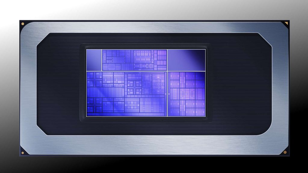
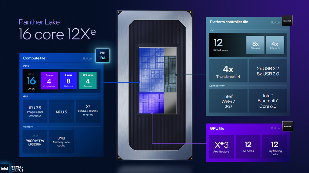
Panther Lake SoCs are all built up from the same cutting-edge P-cores, E-cores, and iGPU architecture, while affording laptop makers more freedom to tailor their products to a wider range of buyers and price points. And as Intel's first product to ship with a compute tile fabricated on the latest 18A process node, Panther Lake has a ton to prove.
At its most recent Tech Tour event, held in the backyard of its leading-edge fabs in Chandler, Arizona, Intel walked us through everything that makes Panther Lake tick. Here’s the story so far.
Intel's 18A process ramps up
Intel's 18A process ramps up
Panther Lake's compute tile is one of the first products to be fabricated on Intel's leading-edge 18A node. As a quick refresher, 18A is Intel's (and likely the industry's) first high-volume process to incorporate two major innovations meant to enable future scaling and power efficiency gains: gate-all-around (GAA) transistors, which Intel calls RibbonFETs, and a backside power delivery network, which Intel calls PowerVia.
(Image credit: Intel)
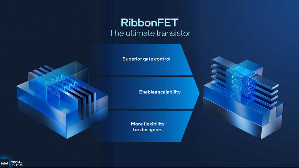
Intel describes its RibbonFETs as "the ultimate transistor," since their gate structure allows for what the company calls "complete control" over the channel. Compared to FinFETs, whose gate structure doesn't extend to the bottom of the channel and therefore has a "weak point" for controlling leakage current, the RibbonFET gate structure entirely wraps around the channel (as defined by the stack of silicon nanosheets at the heart of the device), minimizing undesirable leakage current when the transistor is off. Among other important characteristics, less leakage current means less energy wasted while a chip is operating.
Intel also claims that RibbonFETs are more flexible for designers than FinFETs. The number of ribbons, as well as their widths, can be adjusted to tailor the transistor's performance characteristics to the needs of a given cell.
(Image credit: Intel)
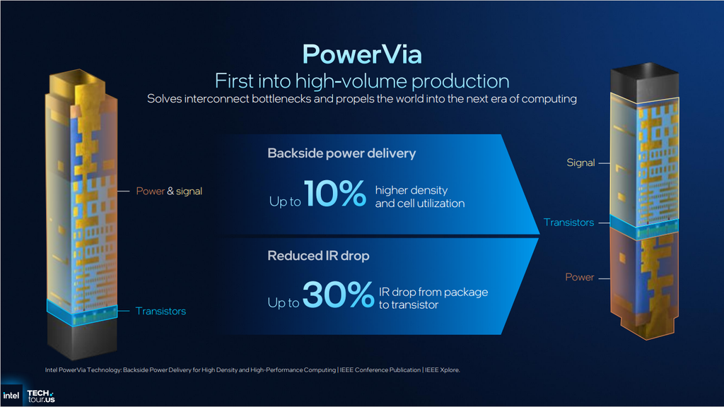
PowerVia, Intel's implementation of a backside power delivery network, introduces a second novel approach to chip fabrication. As silicon processes have gotten denser and denser, efficiently routing both signal and power wires above the transistors has gotten more and more challenging as those wires compete for ever more precious real estate.
Instead of building up both power and signal wires above the transistor, the backside power delivery approach first creates the transistors and signal wiring on the front side of the wafer. In the next production step, the wafer gets flipped over, and the back side gets polished away until the transistor contacts are revealed. The power delivery metal layers are then connected directly to the transistors.
Intel says that PowerVia allows for 10% higher density and relaxed routing on the front side of the wafer. For power delivery, the back-side metal layers reduce power loss from the package to the transistor by 30%.
All in all, 18A allows for a 15% higher frequency at the same power as Intel 3 and a 1.3x density improvement compared to the same process. Designers can also choose to harness 18A's advances to deliver a 25% power reduction at the same performance level compared to Intel 3.
Cougar Cove P-cores and Darkmont E-cores: evolution, not revolution
Cougar Cove P-cores and Darkmont E-cores: evolution, not revolution
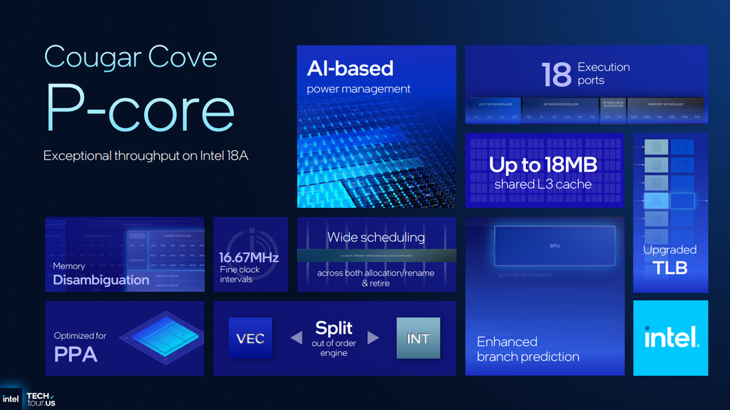
Intel didn't go into fine detail on the changes it made to the Cougar Cove P-core on Panther Lake versus Lunar and Arrow Lake's Lion Cove, or Panther's Darkmont E-core versus Skymont. The improvements the company did discuss for the Cougar Cove P-core are typical refinements of an existing CPU architecture, such as an improved branch predictor and a more capacious translation lookaside buffer (TLB). As Intel says, "we didn't go in and change the width, we didn't change the depth, we optimized."
(Image credit: Intel)
At a high level, Intel says that Cougar Cove now employs an "AI-based" power management approach that can adjust the aggressiveness of certain functional units, such as the prefetcher, on the fly in response to the demands of diverse workloads.
Another change in Cougar Cove is improved prediction behavior in some cases of memory disambiguation. As Intel puts it, when a processor is executing a program, it will perform load and store instructions for memory accesses; sometimes those instructions are connected. Cougar Cove has improved logic to predict when a load and store are connected and use that information to schedule the load correctly. When this prediction is correct, it can result in higher IPC.
Intel also notes that the move to the 18A process gave it the ability to grow some fundamental structures in Cougar Cove, and the TLB was one of the primary beneficiaries. A bigger TLB means that more complex workloads run faster and more reliably, according to Intel.
Cougar Cove also carries forward and refines branch prediction changes introduced with Lion Cove in Lunar Lake. Lion Cove featured improved branch prediction algorithms and delivered low-latency predictions even for branches far ahead in the instruction stream. Intel says Cougar Cove incorporates lessons it learned from shipping Lion Cove silicon to improve performance. It refined some branch prediction algorithms and grew the sizes of each level in the predictor to further lower latency. Cougar Cove can also store better metadata about past prediction results to improve accuracy.
Intel says this all means the Cougar Cove branch predictor can deliver lower latency, more prediction bandwidth, and higher prediction accuracy. These improvements positively impact energy efficiency and performance— a more accurate and more responsive predictor means the CPU core spends less time doing wasteful work and more time doing useful work.
(Image credit: Intel)
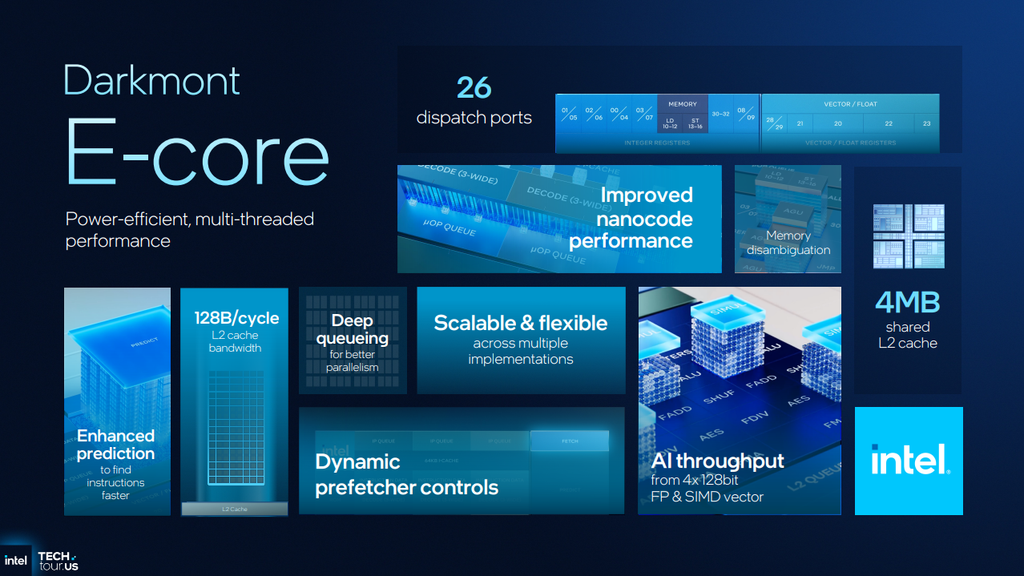
Improvements in the Darkmont E-core are also largely evolutionary versus Lunar Lake’s Skymont. As with Cougar Cove, Darkmont can now use a dynamic algorithm to adjust the aggressiveness of its prefetcher to better balance responsiveness and power efficiency in response to the demands of varying workloads.
Like Cougar Cove, Darkmont offers improved branch prediction accuracy. It also saves power in the front end by employing loop stream detection, a technique that allows the front end of the chip to power down during certain instruction sequences. Darkmont also broadens the cases where the chip can employ nanocode sequences to execute complex instructions that traditionally would have been handled by an x86 CPU's microcode engine. Nanocode was introduced in Skymont to improve both performance and power efficiency.
As Intel puts it, the microcode sequencer is a giant ROM that comes into play when certain complex x86 instructions need to be executed. Loading from that ROM is a serial process, and it can only service one decoder at a time, meaning that other front end units will be blocked if they were also to need instruction sequences from the microcode ROM at the same time. Nanocode prevents this blocking behavior by taking some of those microcode instructions and embedding them into programmable logic arrays in each of the three front-end decoders of the E-core.
Since those PLAs are present in each of the three front-ends of the Darkmont core, Intel says the core can run instructions that formerly resided in microcode as "parallel, out-of-order microcode-like sequences." Intel says Darkmont has more cases and more optimized cases where its front-ends can employ nanocode and leave the microcode sequencer alone.
Mix and match
Mix and match
Not every part of a Panther Lake SoC uses 18A, of course. Intel uses the same "disaggregated architecture" concept that debuted in Meteor Lake and was refined on Lunar Lake and Arrow Lake. This approach separates different functional units of an SoC into individually fabricated "tiles" that are made in Intel's own fabs or at foundries like TSMC, then joined together using Intel's Foveros packaging technology.
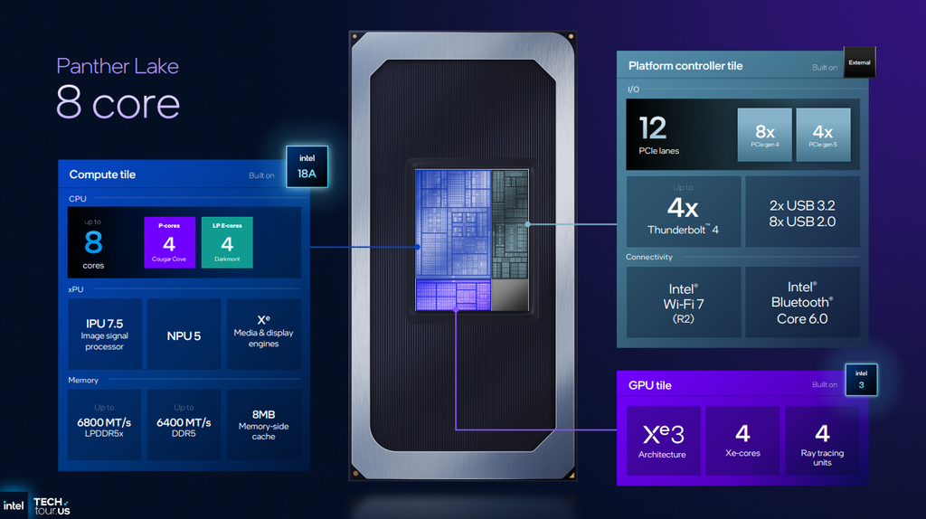
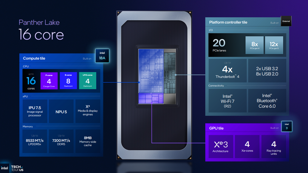
In turn, each Panther Lake compute tile, fabricated in-house on 18A, is built up from three basic core complexes. A compute tile can (so far) include up to four Cougar Cove P-cores, up to eight Darkmont E-cores, and a separate "low-power island" cluster of four more Darkmont E-cores that are meant to "confine" suitable workloads to a lower-power compute domain for extra battery life, an idea introduced in Meteor Lake and refined further in Lunar Lake.
Meteor Lake and Arrow Lake both relied on a pair of Crestmont E-cores in this island that were limited in both power and clock speeds to maximize energy savings, but their limited performance meant that more power-hungry parts of the chip might be awakened more often if a task exceeded their limited capabilities. Lunar Lake got four Skymont E-cores in this island with their own power rail, which allowed them to be clocked higher and do more demanding work before tasks had to be shifted to the P-cores on that SoC.
As an evolution of Skymont, Panther Lake's Darkmont low-power E-cores allow more demanding tasks to stay confined to the low-power island for longer, and they can contribute to multi-threaded workloads for extra parallelism when it's needed. They're not on the main ring bus that connects the main clusters of P- and E-cores on the Panther Lake SoC, however, so they don't share the L3 cache of the larger core cluster. Instead, they have access to a power-efficient 8MB "memory-side cache" that's shared with all the other compute agents on the tile.
This side cache is coherent with the rest of the cache hierarchy across the chip, and coherence among all the caches on Panther Lake is managed by a home agent that communicates with separate coherency agents on each compute domain.
The 18A compute tiles also include Intel's fifth-generation NPU, seventh-generation image processing unit (IPU) for use with premium webcams in laptops, and Xe media and display engines separated from the graphics tile.
For more information on the Xe3 graphics architecture and the two iGPUs that use it on Panther Lake, as well as software and power management improvements, check out our dedicated article.
Three's a crowd
Three's a crowd
(Image credit: Intel)
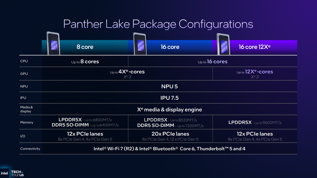
So far, Intel has created two different 18A compute dies that it mixes and matches with two different integrated GPUs (and possibly two different I/O tiles) to create three distinct Panther Lake SoCs, each with different cost and performance targets.
The smallest Panther Lake SoC has four P-cores paired with four low-power E-cores, just like we saw with Lunar Lake. Intel didn't disclose the full specs of its cache hierarchy, but since it lacks higher-power E-core clusters with their own L3 cache, our educated guess is this chip likely only has 12MB of cache shared across its four P-cores. It includes a small Xe3 GPU that offers up to four Xe3 graphics cores. This chip can use traditional DDR5 SO-DIMMs or LPCAMM modules at speeds up to 6800 MT/s, or soldered LPDDR5X running at up to 6400 MT/s.
(Image credit: Intel)
For storage and peripheral controllers, the platform controller tile on the baby Panther Lake SoC offers 12 PCIe lanes - four Gen 5 and eight Gen 4 - which is enough to connect a Gen 5 SSD and perhaps lower-end storage devices or a discrete GPU. Between its relatively low core count, modest graphics horsepower, and limited memory speeds, we're likely to see this chip in more entry-level laptops that prioritize light weight and battery life over absolute performance.
The midsize Panther Lake SoC adds eight E-cores on a ring bus shared with the four P-cores, in addition to the four low-power E-cores in their dedicated island. Intel says this compute die has up to 18MB of shared L3 across the P- and E-cores. This midsize SoC keeps the same 4 Xe Core graphics tile as the small SoC.
(Image credit: Intel)
This chip can take advantage of faster memory than its smaller sibling. Like the small chip, it can use both DDR5 modules or soldered LPDDR5X, but it supports DDR5 at speeds up to 7200 MT/s and LPDDR5X at up to 8533 MT/s.
The midsize Panther Lake chip also has expanded PCIe connectivity from its larger platform controller tile: as many as eight PCIe Gen 4 lanes and 12 Gen 5 lanes. Intel wouldn't comment on particular Panther Lake OEM designs in the pipeline, but between its expanded compute resources, richer PCIe connectivity, and support for higher-speed memory versus its smaller sibling, this chip seems well-suited for pairing with a discrete GPU in thin and light laptops, an approach that some Intel partners took with Meteor Lake chips.
(Image credit: Intel)
The largest Panther Lake SoC retains the same 4P+8E+4LPE CPU core configuration as the midsize SoC but adds a much larger and more powerful 12 Xe3 Core GPU to the package. Intel restricts the memory options that partners can employ with this chip, likely so that it can get adequate memory bandwidth to feed all of those GPU execution units. It can only use LPDDR5X memory and supports the fastest transfer rates of any Panther Lake product: up to 9600 MT/s.
This big chip drops back to the more limited I/O tile with eight PCIe Gen 4 and four PCIe Gen 5 lanes, which is likely an indication that it's targeted at the exploding handheld gaming market and premium thin-and-light laptops that can still game when needed. Pairing discrete GPUs with this version of Panther Lake doesn't make a ton of sense from a system design standpoint.
Performance projections
Performance projections
(Image credit: Intel)
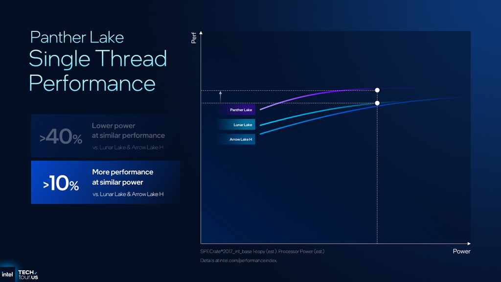
Intel offered a high-level preview of single-threaded performance with Cougar Cove, suggesting that the new P-core can deliver 10% higher performance at similar power to Lunar and Arrow Lake, or 40% lower power at similar performance in less demanding workloads.
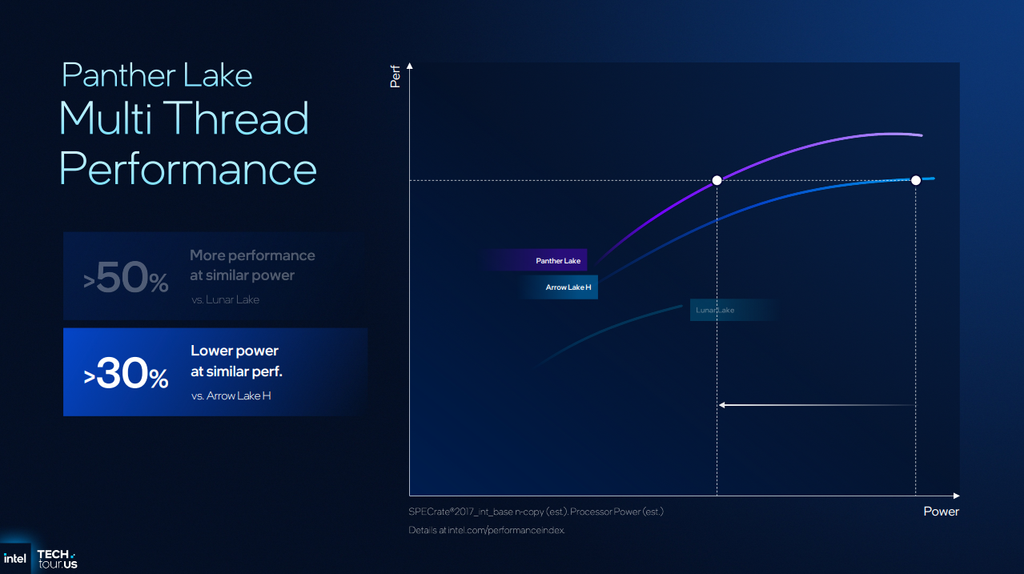
The multi-threaded performance story for Panther Lake is a bit muddier. Intel claims that Panther Lake can deliver 50% more performance at similar power to Lunar Lake, or 30% lower power for multi-threaded performance similar to Arrow Lake-H.
(Image credit: Intel)
Of course, if we consider these charts in their entirety, Panther Lake can also deliver higher absolute performance at similar power to Arrow Lake-H, emphasizing the greater performance scalability of what we assume to be the 4P+8E+4LPE package.
Beyond these broad and rosy performance projections, Intel didn't discuss any specifics on clocks or power targets for Panther Lake during its presentations, but as with any modern laptop SoC, the frequency, power and thermal targets for these chips are likely to cover such a broad range of designs that it's hard to make generalized statements about their performance, and that's before we get into individual chip models within the product stack.
We'll have to wait and see what types of systems Intel's partners typically produce with Panther Lake SoCs inside before we can even begin to establish performance ballparks. Intel says that the first Panther Lake chips will ship before the end of 2025, and that it expects broad market availability starting in January 2026. Given that timeframe, it's probably safe to say that we will hear much more about Panther Lake products at CES.
-
 C114 Communication Network
 -
 Communication Home
