

(Image credit: Intel)
Intel's struggles did not start yesterday, but years ago, and now the company faces problems across multiple fronts. It's hard to say when things turned dark for Intel or attribute any particular business decision that led to this situation, but yet here we are: Intel is bleeding money, the performance of its products is behind offerings from AMD and Nvidia, its foundry efforts yet have to take off as its current process technologies are behind products fabbed at TSMC, and it has to lay off tens of thousands of employees to cut costs and attempt to break even in 2026.
Fabs: Money losers, or key to success?
Historically, CPU design and manufacturing might have been instrumental to Intel's success, but today, the Intel Foundry unit bleeds billions of dollars every quarter, whereas the company's flagship client CPUs are produced by TSMC. Making chips internally almost automatically pushes gross margins to over 50%, unless Intel starts a price war and offers huge discounts to maintain market share. This is, unfortunately, what is happening at Intel at this point, but we'll dive into that topic a bit later.
(Image credit: Intel)
Intel's manufacturing and real estate assets cost around $108 billion, so Intel cannot just offload them to a consortium of investors. Furthermore, the majority of Intel's fabs can only be used to make Intel's own products developed by the company itself. Currently, only select facilities that use Intel 3 and Intel 18A process technologies can be utilized by the company's foundry clients. Other manufacturing processes currently used by Intel are not compatible with industry-standard electronic design automation (EDA) tools, so only Intel's engineers can develop products for these technologies using proprietary EDA software.
There is another thing to keep in mind about Intel's existing production facilities: these are low-mix/high-volume fabs tailored to make Intel's CPUs. These fabs are configured for maximum throughput of a single process flow and product family. Tools are dedicated and duplicated at bottlenecks to sustain high utilization; they run stable recipes for months without change. Also, the production lines are designed so that wafers move continuously with almost no buffers (i.e., waiting areas), and metrology tools are set up to monitor just one specific process in real time. Essentially, Intel's fabs are designed to minimize cost per wafer through efficiency and scale. However, these fabs are not exactly flexible.
Foundries — such as TSMC — run high-mix/low-volume fabs that are built for flexibility to serve many customers and product types. These fabs often use tools that store a wide range of process recipes and can switch between them quickly. Their layouts have staging buffers to manage different types of work-in-progress (WIP), and the automated material handling system (AMHS) is programmed for more flexible routing. They also have more metrology and inspection capacity to handle the greater variation between products, and tool redundancy is spread across many types of equipment to support different process flows. While this setup reduces tool utilization and increases cost per wafer, it enables quicker customer turnaround and supports a wider variety of products.
The key difference between Intel and TSMC is that Intel fabs operate like dedicated high-speed assembly lines, sacrificing flexibility for peak throughput and efficiency, while TSMC fabs function more like flexible manufacturing cells, accepting some efficiency loss in exchange for rapid reconfiguration and multi-product capability.
We do not know whether Intel's 18A-capable fabs in Arizona are low-mix/high-volume facilities or high-mix/low-volume facilities, but this is certainly the case with Intel's pre-IDM 2.0 philosophy and existing fabs. Now that we mentioned Intel's philosophy, it is time to talk about Intel's process technologies.
18A: A turnaround process technology?
Intel's former chief executive Pat Gelsinger touted 20A (2nm-class) and 18A (1.8nm-class) process technologies as production nodes designed for both internal products as well as for third-party foundry clients. Eventually, it turned out that foundry customers had little interest in 20A, so the company decided not to use its Alder Lake products as a pipe cleaner, but to instead produce compute chiplets for these CPUs at TSMC and cancel 20A entirely. This decision put 18A into the focal point as Intel's 'turnaround' node meant for breakthrough Panther Lake and Nova Lake CPUs, as well as external clients.
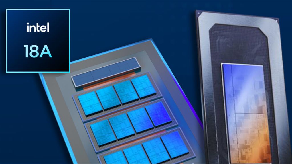
(Image credit: Intel)
Indeed, Intel says that it is on track to produce compute chiplets for its Panther Lake processors later this year at its Fab 52 and Fab 62 in Arizona and perhaps some volume at Fab D1X in Oregon. In addition, Microsoft is committed to using Intel's 18A for some of its upcoming data center designs, and the U.S. Department of Defense plans to use the technology to make advanced processors for aerospace and military applications. Also, Broadcom and Nvidia (probably just like a bunch of other fabless chip designers) are reportedly exploring 18A and 18A-P, but without making any commitments.
Relatively low interest in 18A may be a reason why Intel management reportedly decided to slow down promotion of 18A among external customers and instead focus on promoting its successor, the 14A node (1.4nm-class). The company has never confirmed the decision, but one of the messages that the management sends is that 18A was not designed to be a foundry node from the ground up, which is why it could be less competitive than TSMC's N2 on the foundry market.
There might be merit in the message. Intel has produced its CPUs in-house throughout its history, so the company's main target when developing new fabrication technologies was performance. Intel started to work on 20A and 18A technologies well before the company outlined its IDM 2.0 strategy in early 2021, so while the technology has a decent process design kit (PDK), is compatible with industry-standard EDA tools, and standardized IP blocks (e.g., SRAM macros, I/O cells, PLLs), it may still be more optimized for Intel's client and data center products rather than for a broad set of application that are made by external clients.
General-purpose process technologies like those offered by TSMC usually come are designed and validated for across a wide range of designs, starting from mobile applications processors and all the way to monstrous AI and HPC processors because the same node will serve dozens of companies with very different needs. This adds overhead in development time, test chip diversity, and third-party collaborations, but ensures broad compatibility and predictable yield for a wide customer base.
By contrast, nodes primarily optimized for CPUs may have specific voltage ranges and frequency targets, fewer validated device variants, fewer third-party IP options, and even narrower process windows. Therefore, to target a broader range of customers, Intel might need to do some additional homework, which may not make a lot of financial sense at this stage of development as 18A is behind TSMC's N2 in terms of time-to-market.
However, if Intel does not land any major 18A customers, how will other potential clients know that Intel's fabrication technologies are competitive with those from TSMC in terms of performance, yield, and costs? Since the company does not abandon its 18A as a foundry offering publicly, it is possible that it may continue to target very spcific clients designs with this node. If the company succeeds with landing a customer or two with its 18A technology, it will both earn money and advertize advantages of its fabrication technologies. If not, it will at least not invest millions in an endeavor that will not pay off.
Nonetheless, even if Intel's 18A does not get many external clients, it will still be used to make Panther Lake, Nova Lake (and this processor seems to be Intel's attempt to get back into enthusiast-grade desktops with a monstrous 52-core offering), and other CPUs in the next several years, which will have a positive impact on Intel's balance sheet.
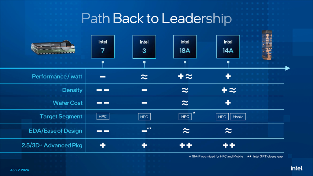
14A: The true foundry node from Intel?
If Intel indeed wants to shift its foundry effort from 18A to 14A, this adjustment may suggest that the company may be repositioning its foundry strategy to leapfrog directly to the next generation, potentially aiming to offer prospective clients a more competitive platform that has been developed as a foundry node from the ground up.
(Image credit: Intel)
However, there is catch with this fabrication technology. Intel recently warned that it is weighing whether to slow down or completely stop work on its 14A manufacturing platform if it cannot secure a large outside client and if development does not meet crucial milestones. This is the first time the company has openly admitted it might step back from leading-edge process technologes, potentially leaving the most advanced production nodes to rivals like TSMC and Samsung. The move reflects a shift toward basing future node development on confirmed commercial demand rather than advancing purely for the sake of technology leadership.
Intel's 14A is an important node for the company not only because it is its first fabrication process developed for foundry customers from the ground up, but also because it will be the first technology to use High-NA EUV lithography for multiple key layers, a leap that requires extremely expensive tools that cost roughly $380 million per unit. Outfitting a fab for high-volume output on 14A would demand tens of billions in equipment purchases (with hundreds of millions for High-NA EUV scanners) on top of billions already spent on process R&D, Intel's executives want to ensure that the effort will pay off. On the one hand, they need to ensure that the technology delivers the right balance of performance and area scaling, on the other hand they need volume commitments from external clients. However, by announcing that it is considering to pull out from the leading-edge semiconductor race, Intel greatly hurts its reputation among potential customers for all of its nodes.
At present, Intel has at least one in-house product planned for the 14A platform, but them management is leaving the door open to outsourcing. If the technology does not move forward, advanced designs that need greater transistor density and speed than 18A-P could provide, they will be manufactured at an outside foundry (i.e., TSMC).
Should Intel shelve 14A and subsequent nodes, the company intends to continue producing the bulk of its portfolio on internal technologies up to 18A-P well into the next decade. This approach would allow Intel to cover most of its needs while avoiding large capital investments for tools and facilities that may go underused. However, relying on outside fabs for top-tier designs could have long-term effects on profitability, especially if those products are key revenue drivers. Essentially, Intel will find itself in a situation similar to today's, only without necessity to invest billions in next-generation tools and fabs.
Intel's current product mix: A bag of hurt?
Right now, Intel's product portfolio is a mixed bag. While the company clearly has some competitive offerings in its mix, its manufacturing strategy leads to profitability woes.
(Image credit: Intel)
On the client side, Alder Lake-S desktop CPUs and Alder Lake notebook parts — both made largely at TSMC — are trailing AMD's Ryzen 9000-series in performance in games, which makes them less competitive in the enthusiast and high-end segments. Several months ago, Intel even admitted that some enthusiasts still prefer 13th Generation Core 'Raptor Lake' processors, which are built in-house and carry a higher margin, but it is an aging design on a less advanced node, so Intel's positions against AMD's Ryzen 9000 cannot be improved significantly in the high-end segment.
Lunar Lake, also fabbed externally, is aimed at thin-and-light notebooks and integrates LPDDR5X memory directly on the package. While this improves power efficiency and simplifies board design, it adds significant bill-of-materials cost and squeezes margins in a segment where pricing pressure is already intense.
For now, Intel is offering two parallel client CPU lines — made internally and externally —neither of which fully satisfies the needs for both performance leadership and profitability.
In the data center, Intel has finally ramped its Xeon 6 family — consisting of Xeon 6000P-series 'Granite Rapids' with high-performance cores and Xeon 6000E-series 'Sierra Forest' with energy-efficient small cores. Both are manufactured internally, which should in theory help with margins. However, the data center and AI (DCAI) group faces unprecedented competitive pressure from AMD's EPYC lineup and to some degree Arm-based solutions, which forces Intel to make discounts at the cost of its margins.
Internal clashes
As if usual challenges with process technology development and competitiveness of product mix were not enough, Intel apparently has internal clashes on the board-of-directors level.

(Image credit: Intel)
Earlier in 2025, Intel board chairman Frank Yeary reportedly explored spinning off Intel Foundry into a joint venture with TSMC and major fabless chipmakers — or even selling its controlling stake outright to TSMC. These proposals were opposed by newly appointed CEO Lip-Bu Tan, which sparked internal friction, as Tan viewed keeping Intel's own fabs as vital for competitiveness and an important factor for the U.S. national security (i.e, so Intel would have a bargaining chip with the U.S. government). While some directors backed Yeary, the spin off did not happen, but the disagreements ultimately undermined Tan's early strategic efforts.
The disputes slowed or blocked several of Tan's plans, including raising billions from Wall Street to boost Intel's manufacturing investments and acquire an AI accelerator developer, according to the Wall Street Journal. As a consequence, prolonged debates allowed a competing tech company to move closer to securing the AI target before Intel could act.
To add to already rather intense situation on Intel's board, it should be noted that TSMC had little (if at all) interest in taking over Intel's manufacturing facilities both because these are low-mix/high-volume fabs tailored for making CPUs and because the companies use completely different process technologies and converting Intel's fabs to TSMC's production methods would barely make financial sense for the company. Given these limitations, the idea was improbable from the start, yet it still became a flashpoint in leadership disputes.
Political pressure
To top Intel's list of pains, U.S. President Donald Trump last week called for Intel CEO Lip-Bu Tan to resign over alleged conflicts of interest tied to his financial holdings in Chinese technology companies, some linked to China's military.

(Image credit: Intel)
Tan, who retains its stakes in over 600 Chinese firms through his venture capital led by Walden International, rejected the accusations in a letter to employees. He wrote that accusations were based on misinformation and stressed his adherence to strict legal and ethical standards. While the Intel board officially expressed full support for Tan, industry sources suggest the criticism may also be driven by internal dissatisfaction over job cuts and clashes on the board level.
To persuade the U.S. President over his loyalty to Intel and the U.S., Lip-Bu Tan plans to talk with Donald Trump on Monday, but we will likely learn about the results at a later time.
Summary
Intel faces deep, multi-front challenges that it must solve to survive.
Intel's client CPU lineup is split between TSMC-made chips with thin margins and older in-house designs that trail AMD in performance, while new Xeon 6 server CPUs face fierce competition and margin pressure. The company's foundry efforts yet have to gain traction as Intel's 18A is behind TSMC's N2 in terms of time-to-market for external custmers and is barely endorsed by major clients. Intel's 14A promises to be a better fit for foundry customers as it was designed as a foundry node from its inception, but to make 14A happen, Intel must land at least one major client to pay off its massive investments.
Unfortunately, Intel faces problems not obly on products and manufacturing facility levels. Internal conflicts on the BoD level have slowed strategic moves, including a proposed AI hardware developer acquisition, and political pressure has mounted after President Trump called for CEO Lip-Bu Tan's resignation over alleged conflicts of interest tied to his Chinese investments.
-
 C114 Communication Network
 -
 Communication Home
